Heterozygosity - definition
Heterozygosity - definition
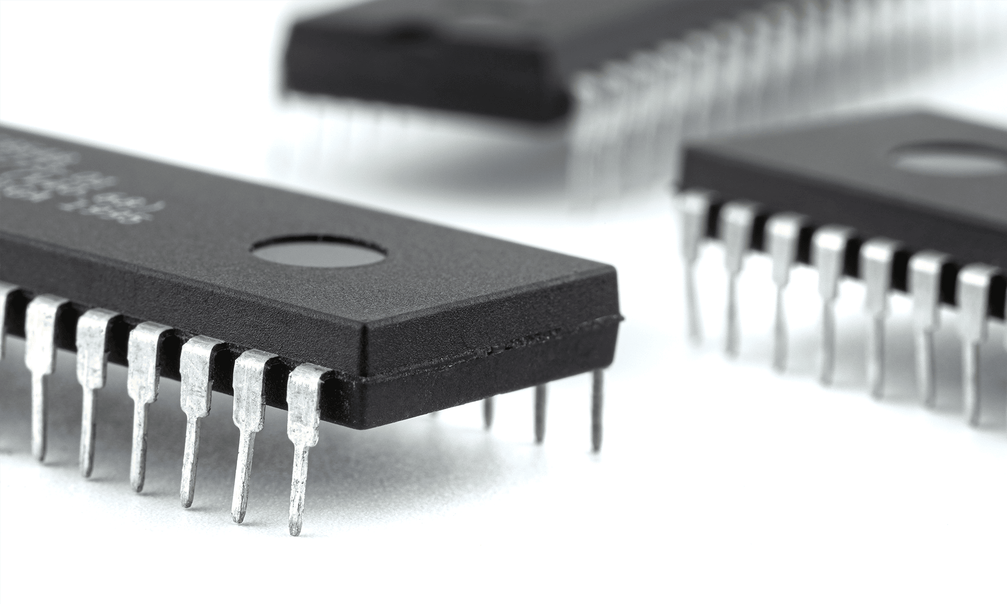
A Heterojunction is the interface between two different semiconductor materials with different physical properties, such as energy gap width, electron affinity or crystal lattice constant. Unlike a classical p-n junction, which is formed within a single material, a heterojunction is formed by connecting two different semiconductors, leading to unique electron phenomena at the interface.
A key effect of the heterojunction is the formation of an energy barrier resulting from differences in the energy band levels of the two materials. This phenomenon is used for the controlled formation of internal potentials, which enables precise control of charge flow in electronic and optoelectronic devices. This makes it possible to achieve structures with exceptional efficiency, speed or sensitivity not possible with homogeneous connectors.
Heterojunctions are widely used in modern semiconductor components such as HEMT (High Electron Mobility Transistor) transistors, semiconductor lasers, light-emitting diodes (LEDs), solar cells and radiation detectors. Precise control of heterojunction parameters is made possible by advanced epitaxy technologies, which allow the growth of thin crystalline layers while maintaining lattice continuity between different materials.
Differences in the properties of the materials in the heterojunction allow the formation of areas of very high electron or hole mobility, resulting in increased charge transport efficiency and lower energy losses. Phenomena occurring at the heterojunction interface are fundamental to the design of high-performance micro- and optoelectronic systems, as well as to the research into new semiconductor materials.
Transfer Multisort Elektronik (TME) is one of the world’s largest global distributors of electronic components, electrotechnical parts, workshop equipment, and industrial automation. The catalog includes over 1,500,000 products from 1,300 leading manufacturers. TME’s modern logistics centers in Łódź and Rzgów (Poland), with a combined area of over 40,000 m², ship nearly 6,000 packages daily to customers in more than 150 countries.
TME also invests in the development of knowledge and skills of young engineers and electronics enthusiasts through the TME Education project, and supports the tech community by organizing the TechMasterEvent series, promoting innovation and experience exchange.