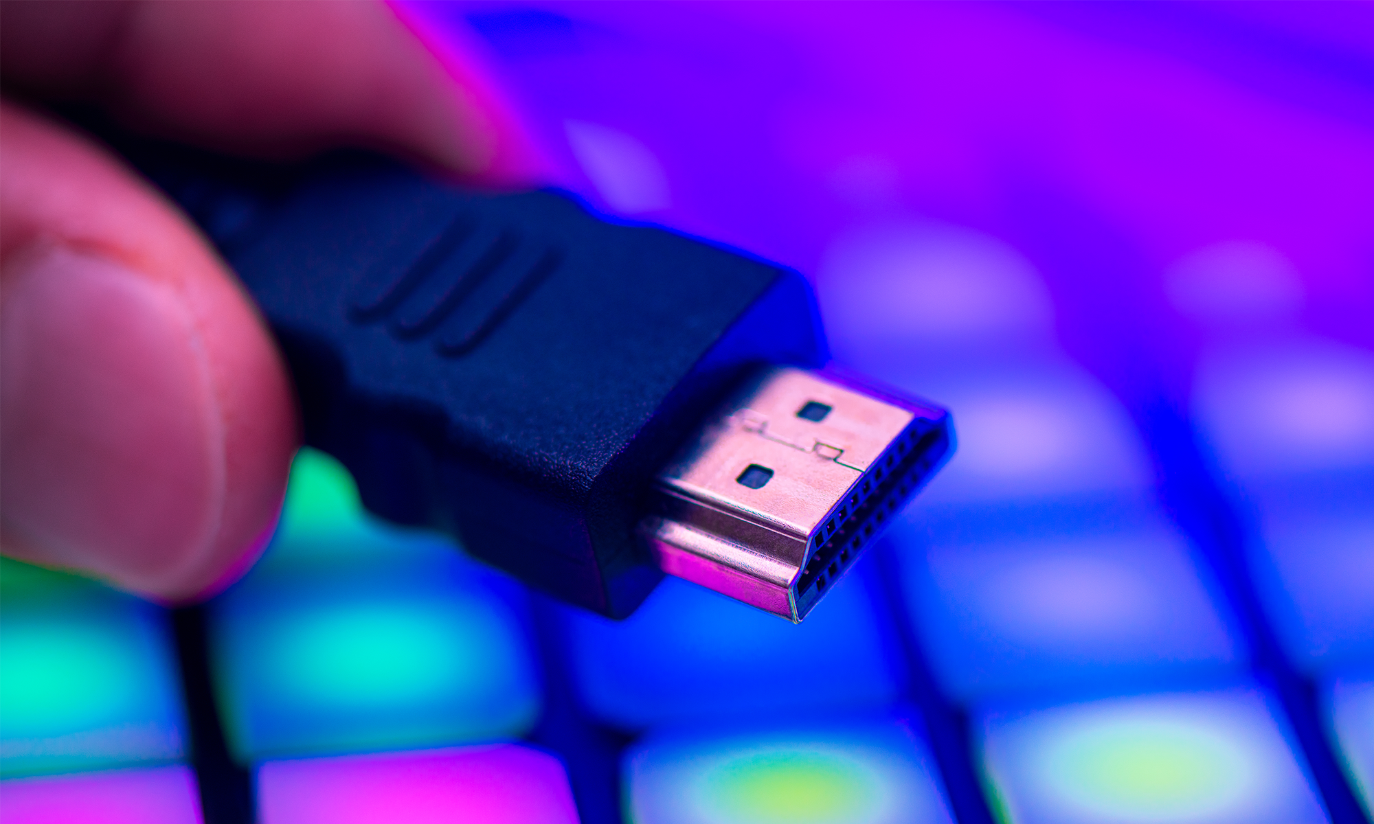
FLASH memory: structure and functioning
FLASH memory: structure and functioningDate of publication: 16-05-2025 Update date: 10-04-2026 🕒 8 min read
FLASH memory is a type of non-volatile semiconductor memory, which means, that it retains data even after power is removed. Unlike the older EEPROM technology, which allowed deletion of single bytes, FLASH memory erases data in blocks, which significantly speeds up write and erase operations. The name "FLASH", meaning "flash", was given to this type of memory because of the speed of the erasing process.
- Structure of FLASH memory
- Operating principle
- Types of FLASH memory
- Performance characteristics
- Applications of FLASH memory
- Challenges and limitations of FLASH technology
FLASH memory plays a key role in today's technological world. It is used in a wide range of devices, from smartphones and cameras to SSDs and automotive systems. Its versatility and reliability have made it, it has become an indispensable part of our daily lives.
The history of FLASH memory dates back to the years 80. XX century, when the company Toshiba developed the first prototype. The technology evolved from EEPROM, offering durable and fast data storage. Since then, FLASH memory has undergone numerous improvements, that have led to increases in its capacity and performance, revolutionizing the way, the way we store and use data.
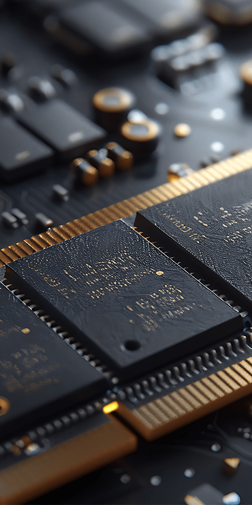
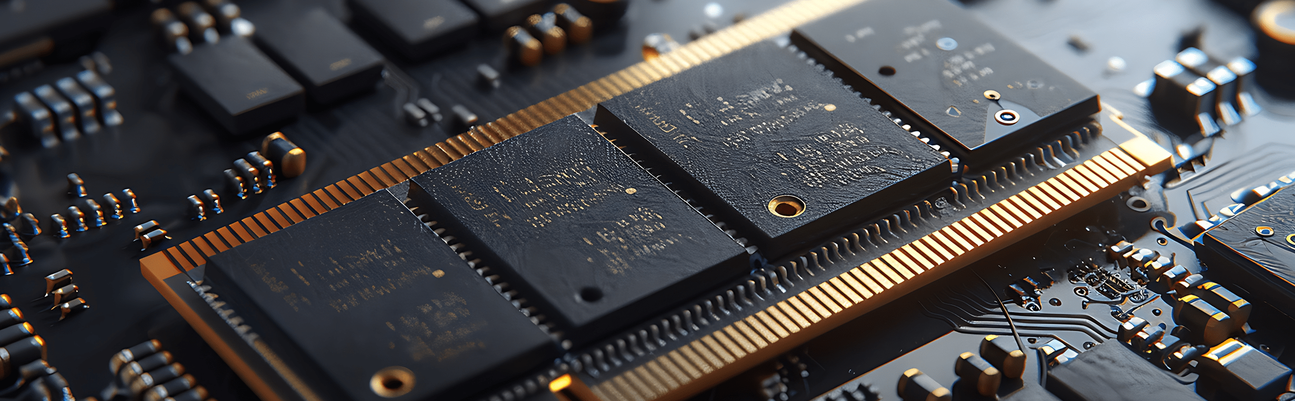
Construction of FLASH memory
FLASH memory, despite its versatility, is based on a relatively simple, but clever design. Its basic element is the memory cell, and the key to its operation is the floating-gate field-effect transistor.
Basic element: the memory cell
At the core of FLASH technology lies the floating gate field-effect transistor (Floating Gate Transistor). The peculiarity of this transistor is that it has an isolated gate, located between the control gate and the conduction channel. This insulated floating gate serves as an electrical charge storage area; the charge accumulated or removed from it determines the logic state of the cell ("0" or "1", respectively).
FLASH memory architectures
FLASH memory cells can be combined in different ways, which gives us two main architectures of FLASH memory: NOR and NAND.
- NOR FLASH
In NOR FLASH, cells are connected in parallel. This design enables fast random reading of data, as well as writing at the single byte level. For this reason NOR FLASH is used in applications, where fast access to program code is crucial, for example, in firmware of embedded devices or BIOS memory of computers. The name "NOR" comes from the similarity of the layout of cell connections to NOR logic gates. - NAND FLASH
In NAND FLASH, cells are connected in series in strings. This organization translates into higher storage density of data, faster sequential writing and block erasing, as well as a lower cost per bit. NAND FLASH is dominant in data storage media, such as SSDs, memory cards or pendrives, where the capacity and efficiency of storing large amounts of data is of primary importance. As with NOR, the name "NAND" reflects the similarity to NAND logic gates.
Physical structure: evolution from 2D to 3D NAND
Initially, FLASH memory cells were laid out flat, forming 2D NAND (Planar NAND). However, miniaturization of technological processes and the drive to increase capacity encountered physical limitations. The answer to these challenges became 3D NAND, in which cells are stacked in layers, one on top of the other. Such a solution has made it possible to break through storage density barriers, as well as to improve the performance and durability of FLASH memory.
Principle of operation (functioning)
FLASH memory allows you to store data thanks to the specific properties of memory cells and the operations, that are performed on them.
- Data storage: the basis of information storage is the presence or absence of an electrical charge in the floating gate of a transistor. The logic state of "0" and "1" is represented by the stored or deleted charge, respectively. Changing the amount of charge in the floating gate directly affects the threshold voltage of the transistor, i.e. the voltage, at which the transistor begins to conduct the current.
- Operations on FLASH memory: FLASH memory performs three basic operations: reading, programming (writing) and erasing.
- Read (Read): the read operation involves measuring the conductivity of a transistor. Put simply, we check, whether at a certain voltage applied to the control gate the transistor conducts current, or not. Based on this, whether current is flowing, or not, we read the logic state of the cell ("0" or "1").
- Programming (Write/Program): writing data, i.e., programming the cell, involves injecting electrons into a floating gate. This process is often implemented using Fowler's quantum tunneling-Nordheim, which allows precise placement of a charge in an isolated gate.
- Erase (Erase): deleting data means removing electrons from the floating gate. In contrast to write, erasing in FLASH memory takes place on entire blocks of cells, rather than on individual cells. This block nature of erasure is the source of the name "FLASH", referring to the speed of "flash" deletion of larger portions of data.
Types of FLASH memory (due to the number of bits per cell)
FLASH memory can be divided into different types, depending on the number of bits stored in a single memory cell. The basic types are SLC, MLC, TLC and QLC.
SLC (Single-Level Cell)
SLC (Single-Level Cell) is a technology, in which 1 bit of information is stored in a single memory cell.
Benefits:
- highest speed of operation.
- highest durability and reliability.
Disadvantages:
- low capacity.
- high cost.
MLC (Multi-Level Cell)
MLC (Multi-Level Cell) is a technology, which allows 2 bits of data to be stored in a single memory cell. MLC represents a compromise between capacity, performance and cost.
TLC (Triple-Level Cell)
TLC (Triple-Level Cell) allows 3 bits of information to be stored in a single cell. TLC offers higher capacity and lower cost, but at the cost of lower performance and durability compared to MLC/SLC.
QLC (Quad-Level Cell)
QLC (Quad-Level Cell) stores 4 bits of data in each cell and has the highest storage density and lowest cost per bit, but also has the lowest performance and durability.
PLC (Penta-Level Cell) and the future
Work is underway on technologies such as PLC (Penta-Level Cell), which will make it possible to store 5 bits in a single cell. Further development in this direction involves prospects for increasing storage density, but also with the challenges of maintaining performance and durability.There are clear relationships between storage density, speed, endurance and cost of FLASH memory. Increasing storage density (the number of bits per cell) is usually associated with a decrease in speed and endurance, but allows for a reduction in cost.
Performance characteristics and reliability
Performance and reliability are the key parameters that characterize FLASH memory.
Read and write speeds
Read and write speeds vary depending on the type of FLASH memory (SLC, MLC, TLC, QLC) and its architecture (NAND vs NOR, 2D vs 3D). SLC memories have the highest speed, and QLC the lowest.In FLASH NOR memory, the cells are organized in such a way that each cell can be directly addressed, which allows data to be read byte by byte (or word by word) without having to load the entire block. NOR memory offers fast, random access to data.In NAND memory, on the other hand, reading/writing is done in pages and blocks of data. NAND memory has higher packing density and lower manufacturing cost, but read/write is done sequentially and requires reading the entire page into the buffer.
Latency
Data access latency is another important performance parameter, which also depends on the type and architecture of the FLASH memory. NOR memory is characterized by low random read latency, which is crucial in applications requiring fast access to small portions of data. NAND memory, on the other hand, due to the sequential nature of access, can have higher latency in random operations, but offers high throughput when reading and writing large blocks of data.
Endurance
FLASH memory has a limited endurance, which means, that each cell can only withstand a certain number of program/erase cycles (P/E cycles). The number of P/E cycles varies for different types of memory and the largest is for SLC, and the smallest for QLC.The SLC cell, switching only between 2 states, is the most durable (greatest tolerance to multiple erasures, because the voltage margins are large). A typical SLC cell lasts on the order of 100,000 P/E (Program/Erase - write/erase) cycles.An MLC cell (2-bit) has four levels - smaller threshold spacing - making read errors more frequent and gate/insulator material fatigue faster. MLC life is typically around 10,000 cycles. TLC (3 bits) is 8 states - even more difficult to distinguish between levels - typical life of about 3,000 cycles. QLC (4 bits, 16 states) has a durability of several hundred to 1-2 thousand. write cycles.
Reliability and data retention
FLASH memory reliability refers to how, how long data can be safely stored without loss of integrity. This time depends on a number of factors, including the type of memory, environmental conditions and the number of P/E cycles. FLASH memory reliability is also affected by error correction mechanisms and wear management techniques, which compensate for the limitations associated with memory cell longevity.
Mechanisms that improve longevity and reliability
Others mechanisms exist, that improve the lifetime and reliability of FLASH memory
- Error Correction Code (ECC)- Error Correction Code)
- Wear leveling (even wear of cells)
- Bad block management (Bad Block Management)
Error correction code (ECC) is a technique, which allows detection and repair of data errors, that can occur when reading from FLASH memory.
Wear leveling is an algorithm, that evenly distributes data writes to all memory cells, in order to prevent excessive usage of some of them.
Corrupted block management involves detecting and excluding corrupted memory blocks from use, which ensures the continued reliability of stored data.
FLASH Memory Applications
FLASH memory, thanks to its unique properties, has found wide application in many fields.
Consumer electronics
FLASH memory is widely used in consumer electronics. It can be found in portable Mass Storage devices, such as flash drives, which are used for easy transfer and storage of data. Memory Cards, including SD formats i microSD, are indispensable in digital cameras, camcorders and MP players3, enabling multimedia recording and playback.
Mobile devices
FLASH memory is a key component of mobile devices. In smartphones and tablets, it serves as the internal memory, on which the operating system, applications, photos, videos and other user data. The dynamic development of these devices and their growing multimedia capabilities have significantly increased the demand for high-capacity FLASH memory.
Personal computers and servers
In personal computers and servers, FLASH memory is used in Solid State Drives (SSD). SSDs offer much faster access to data, faster system and application boot times, and greater resistance to mechanical damage compared to traditional hard drives. In servers and data centers, SSDs increase the performance of input/output operations, which is crucial for handling heavy workloads and providing fast data access.
embedded systems
FLASH memory is also used in embedded systems (Embedded systems). Embedded systems are specialized computers, that are an integral part of various devices and machines, such as household appliances, industrial equipment, and even toys. In these systems, FLASH memory is used to store firmware, configuration data and other relevant information.
Motorization (Automotive)
In automotive applications, FLASH memory is used in infotainment systems, navigation and data recorders. Infotainment systems provide entertainment and information to the driver and passengers, navigation systems store maps and route data, and Recorders record data from the vehicle's sensors, which is important for accident analysis and monitoring vehicle performance. FLASH memory in automotive applications must be characterized by high reliability and resistance to extreme temperature conditions and vibration.
Industrial and scientific applications
FLASH memory also has wide applications in industry and science. In industry, it is used in machine controllers, monitoring systems and measuring devices. In science, it is used to store data from experiments, configuration of laboratory equipment and archiving of test results. In these applications, durability is key, reliability and resistance to harsh environmental conditions.
Telecommunications and Networks
FLASH memory is used in telecommunications and networks. In network devices, such as routers and switches, it is used to store system software, configurations and logs. In telecommunications, FLASH memory is used in telephone exchanges and data transmission systems.
Data Centers (Data Centers)
FLASH memory plays an important role in data centers. SSDs, based on FLASH memory, are used to store data, to which fast access is required. FLASH memory speeds up database operations, transaction processing and data analysis, which is crucial for efficient operation of web and cloud services.
Challenges and limitations of FLASH technology
Despite its many advantages, fLASH technology also faces some challenges and limitations, that affect its development and application.
Limited durability
One of the key problems is the limited lifetime of FLASH memory, resulting from the wear and tear of memory cells during write and erase cycles. Each FLASH memory cell can only withstand a certain number of such cycles, beyond which it begins to lose its properties, which may lead to data loss. SLC memories are characterized by greater durability, but are more expensive and less capacious, while MLC, TLC and QLC offer higher capacity at the expense of durability.
Performance degradation
FLASH memory performance can decline as the memory fills up and as wear and tear progresses. Writing data to partially filled memory requires the FLASH controller to perform additional operations, such as moving data and erasing blocks, which increases the write time. Similarly, wear and tear on memory cells over time increases vulnerability to errors and requires more intensive use of error correction mechanisms, which also affects overall performance.
Data security
Data security is another important aspect of FLASH memory, like any data carrier, is exposed to the risk of data loss due to hardware failure, software errors or malware attacks. In addition, in case of theft or loss of a device containing FLASH memory, data can get into the wrong hands. Therefore, in order to protect confidential information, it is recommended to use data encryption.
Production costs
FLASH memory production costs, especially with the latest technologies such as 3D NAND, can be high. The manufacturing process of 3D NAND structures is more complicated and requires advanced manufacturing technologies, which translates into higher costs. Nevertheless, technological advances and increasing competition in the market are contributing to a gradual reduction in the price of FLASH memory.
Summary and the future
In this article, we discussed key aspects of the structure and operation of FLASH memory. We looked at the structure of a memory cell, based on a floating gate transistor or charge trap, and the principles of writing and reading data, involving controlling the flow of electrons. We explained the differences between NOR and NAND architectures, and we also discussed the evolution of cell technology from SLC through MLC, TLC to QLC.
FLASH technology has had a revolutionary impact on the way data is stored, by making it possible to create fast, energy-efficient and compact storage media. From Memory Cards in digital cameras to SSDs in computers, FLASH memory has become an indispensable part of modern electronics.
Directions for FLASH technology include further advances in 3D NAND, allowing for increasing data packing density and lowering costs, the drive to increase the number of bits stored per cell (e.g. PLC), the search for new materials and improvements in memory management algorithms.
The role of FLASH memory in the future of technology appears to be unthreatened. It will continue to be crucial in the development of artificial intelligence, cloud computing, automotive, as well as in many other areas, where fast access to data and reliable storage are essential.
Transfer Multisort Elektronik (TME) is one of the world’s largest global distributors of electronic components, electrotechnical parts, workshop equipment, and industrial automation. The catalog includes over 1,500,000 products from 1,300 leading manufacturers. TME’s modern logistics centers in Łódź and Rzgów (Poland), with a combined area of over 40,000 m², ship nearly 6,000 packages daily to customers in more than 150 countries.
TME also invests in the development of knowledge and skills of young engineers and electronics enthusiasts through the TME Education project, and supports the tech community by organizing the TechMasterEvent series, promoting innovation and experience exchange.