Miller effect and its impact on amplifier systems
Miller effect and its impact on amplifier systemsDate of publication: 10-07-2024 Update date: 10-04-2026 🕒 5 min read

The common definition of the “Miller effect” refers to the situation in which the capacitance between the input and output terminals of the inverting amplifier is transferred (sometimes as a much amplified value) to its input. This effect impacts not only capacitance, but also any type of impedance connected to the amplifier feedback node. This phenomenon was initially described in 1920 by John Milton Miller in relation to a vacuum tube amplifier, i.e. “Thus the apparent input capacity can become a number of times greater than the actual capacities between the tube electrodes…” .
- How is the Miller effect generated?
- How can the Miller effect be mitigated?
- How can the Miller effect be used in practice?
What the Miller effect is and how it occurs
Before we get down to explaining how the Miller effect is generated and what its impact on the amplifier system is, we will analyse an example that will make it easier for you to understand it almost intuitively. Figure 1. presents a typical transistor amplifier configured with a common emitter. For the sake of simplicity, base polarising components (i.e. components establishing the transistor operation point) have been omitted. The figure shows stray capacitances present in the amplifier. The CBE capacitance is present between the transistor base and ground, and the CCE capacitance occurs between the collector and ground. And what is the collector-base capacitance designated as CCB?
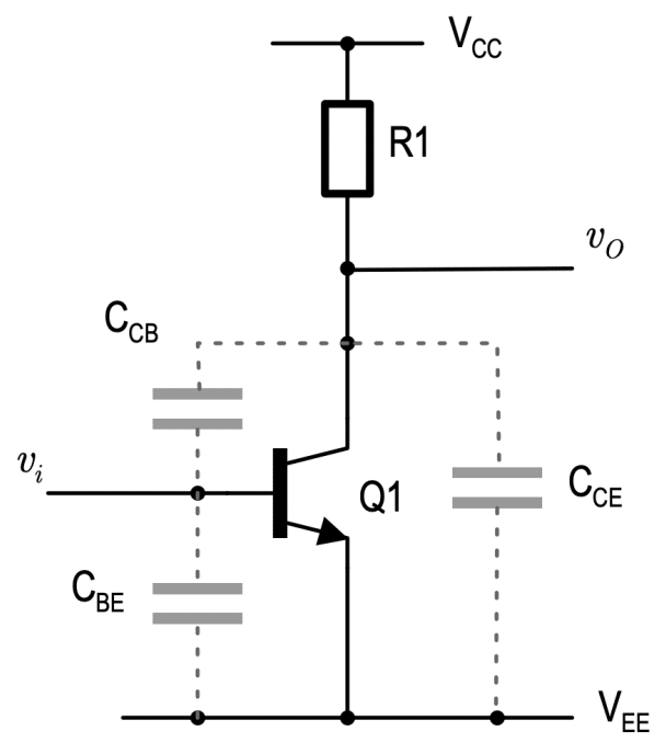 Figure 1. Stray capacitances in an OE amplifier
Imagine that, in the amplifier input in Figure 1, there is a slight positive voltage, which polarises transistor Q1 in the forward direction. As we are dealing with an inverting amplifier, there will be a voltage drop at the transistor collector, which, due to the amplifier gain, will be significantly greater than the input voltage. The voltage present on the CCB stray capacitance capacitor plates is UCB = vi (1 + KU), where KU is the voltage gain. The current flowing through the CCB capacitor is increased by the same factor. It is equivalent to the situation in which the CCB capacitance “moves” to the amplifier input and connects in parallel with the CBE input capacitance.
Semiconductor manufacturers strive to keep stray capacitances as small as possible. In low-power transistors, they typically amount to a few pF, but as the stage gain is required, this effect can become significant in relation to the circuit operation.
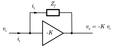 Figure 2. The ideal inverting amplifier
Figure 2 presents a general overview of an ideal inverting amplifier. It comes with gain K and is included in the feedback node with impedance Zf. The input current ii can be determined using the following formula:
The input impedance for this system can be determined using the following formula:
Note that the input impedance is smaller than the feedback impedance by 1+K. This is the same result as the one obtained at the beginning of this text (i.e. the intuitive example), as long as we know (or remember) that a lower input impedance is matched by a higher capacitance that occurs in it.
Miller effect mitigation
When we already know why this phenomenon occurs, we can consider how its impact on amplifier operation can be mitigated. We can also work out the negative results of the Miller effect occurrence. Most of all, it reduces the gain as the input signal frequency increases, thereby limiting the frequency response. In switching systems, such as DC/DC converters, the Miller effect decreases the control signal edge steepness, reduces the inverter energy efficiency, and increases the requirements for the transistor stage controlling driver.
How can we handle the Miller effect in an amplifier? The easiest approach is to create an amplifier control stage with a very low output impedance, so that the stray capacitance gets loaded very quickly, and, as a result, its impact on the amplifier operation is negligible. Even if we are dealing with a low-performance source, an additional buffering stage can be provided at the amplifier input. Another obvious method involves reducing the amplifier stage gain. However, it can result in a necessity to combine multiple stages to achieve the intended gain and thus increase the amplifier noise.
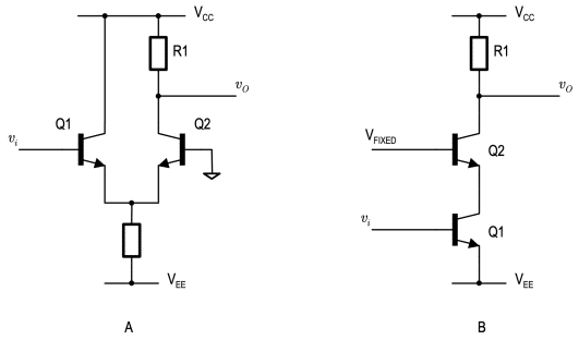 Figure 3. Differential amplifier and cascode amplifier that limits the Miller effect
Using a differential amplifier or a cascode amplifier is a good idea. Figure 3. presents general diagrams of such solutions. Figure 3a shows an amplifier with a differential pair. There is no resistance in the collector circuit of transistor Q1, so the collector voltage is constant, which means that there is no Miller effect. The Miller effect does not occur in transistor Q2 either, as it base is connected to the ground, which results in the smallest possible source impedance. Figure 3b shows the cascode amplifier circuit in which base Q2 is polarised with the constant voltage from the source (the base polarisation method is omitted). The voltage of emitter Q2 is lower, by the value of the VBE decrease, than the base polarisation voltage. The collector of transistor Q1 shows constant voltage, so the Miller effect cannot occur. The current of collector Q1 flows through Q2 and load resistor R1, similarly to a typical OE amplifier.
The Miller effect occurrence is not limited to discrete circuits. It also occurs when an integrated amplifier is used, as long as capacitance, resistance or inductance is included in its feedback node, so practically in every situation where an amplifier is used. A device designer must always be aware of this phenomenon and limit its impact, if necessary.
The Miller effect increases together with the increase in stray capacitances. To put it simply, the bigger the transistor and the higher the current it conducts, the higher the stray capacitance. Therefore, this phenomenon cannot be ignored when it comes to building devices with high-power IGBT or MOSFET transistors. Its impact is even more significant for vacuum tube amplifiers in which the stray capacitance values for tube electrodes are very high.
Using the Miller effect in practice
The Miller effect is not just a problem that must be solved to ensure proper system operation. In fact, it has a range of applications in electronic engineering and telecommunications, as it can be used to build filters, shape the circuit transmission characteristics, and its impulse response. Among others, the Miller effect is used while designing oscillators, high-speed data transmission systems, in RF and microwave applications, buffer amplifiers, measurement amplifiers, power amplifiers, or to stabilise the gain and impulse response of feedback nodes, for signal conditioning and other applications.
Transfer Multisort Elektronik (TME) is one of the world’s largest global distributors of electronic components, electrotechnical parts, workshop equipment, and industrial automation. The catalog includes over 1,500,000 products from 1,300 leading manufacturers. TME’s modern logistics centers in Łódź and Rzgów (Poland), with a combined area of over 40,000 m², ship nearly 6,000 packages daily to customers in more than 150 countries.
TME also invests in the development of knowledge and skills of young engineers and electronics enthusiasts through the TME Education project, and supports the tech community by organizing the TechMasterEvent series, promoting innovation and experience exchange.