Laminates and prototype PCBs
Laminates and prototype PCBsDate of publication: 10/25/2023 Update date: 04/10/2026 🕒 12 min read
The ‘DIY’ PCB making techniques are not at all reserved for hobbyists only – they are also used by professionals and small manufacturers, especially for PCB prototyping.
Highlights at a glance
-
Laminates are the primary material in printed circuit board (PCB) manufacturing.
-
Popular technologies for creating PCBs include CNC milling and chemical etching.
-
CNC milling offers high precision and mechanical strength to the PCB.
-
Traditional etching uses a chemical reaction to remove copper, but requires a precise protective layer.
-
Phototransfer technology allows professional precision even at home.
-
Photosensitive Laminates enable highly accurate transfer of the circuit image.
-
Specialty Laminates are available, such as. with an aluminum layer for heat dissipation.
-
Universal PCBs speed up prototyping with ready-made tracks and solder fields.
-
Contact boards enable rapid prototyping without soldering.
-
TME products are aimed at both professionals, electronics professionals and amateurs.
The TME offering is addressed to large companies and small manufacturers or service centers alike, as well as to students, and even amateurs. All of them will surely appreciate the wide selection of universal PCBs, laminates and other products for the prototyping of electronic devices.
This articles covers topics such as:
Copper laminates
Individual PCBs are made using laminates, i.e. sheets of plastic (usually epoxy glass) that are factory-coated with a homogenous layer of copper. Traces, solder pads and other PCB components are made by removing the conductive layer chemically or mechanically. The former technology is the so-called etching (more about it later), while the latter one involves the use of a CNC machine. There, a digitally controlled milling machine removes the copper so that only a computer-designed PCB layout is left on the laminate surface. For this kind of processing, adequately sized material is required – a thicker laminate board will be the optimal choice as it will provide tolerance in terms of the milling depth and, in addition, retain mechanical resistance (even if processed on both sides). The products available from the TME catalogue are up to 2.4 mm thick, so the customers will surely find the right items for their needs.
 Making a PCB with the use of a CNC milling machine.
‘Classic’ etching
PCB etching makes use of chemical reactions. One of the most popular methods is the oxidation of copper using sodium persulphate. Before immersing the PCB in the solution, the layout of the circuit is applied onto the board with the use of an insoluble substance that protects metal fragments from coming into contact with the etching agent.


There are several technologies for applying the protective layer. In fully amateur conditions, a toner transfer from a laser printout is used. Sometimes (in the case of the simplest circuits), drawing the traces with a special marker pen is enough. Both methods can produce satisfactory results, but their accuracy is limited. Any laminate (even 0.6 mm) can be used for such work, but the thickness of the copper layer has to be taken into account (there are products where this value ranges from 18 µm to 105 µm). The more solid the metal layer is, the longer the etching process will take, and such prolonged immersion in the solution may cause damage (‘over-etching’) to the smallest parts of the layout, e.g. narrow traces.
‘Photo-transfer’
Electronic components are getting increasingly smaller, and some of them are only available in SMD packages. Nowadays, not only electronic device manufacturers, but also amateurs feel the need to make precise circuits characterised by tolerance of a few dozen, or even just a few micrometres. This is why the photo-transfer technology, which allows to achieve almost professional results – but without the use of a specialist machinery – is becoming increasingly popular.
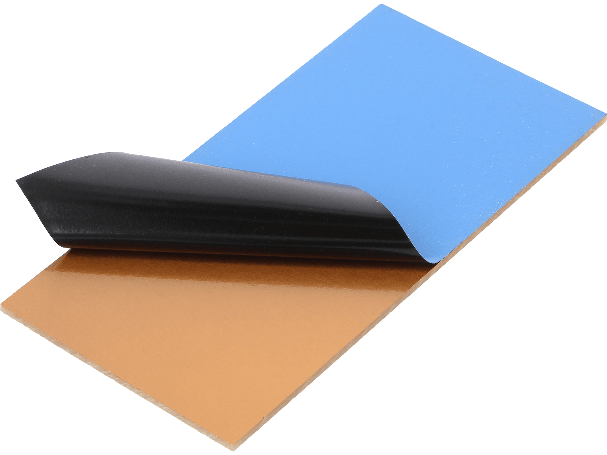 Film-protected photoresist-coated laminate.
Photo-transfer does not refer to a method of making PCBs as such (traces are made by etching, as described above) – but to a technology of applying a protective layer to the laminate. First, the copper is coated with a photosensitive substance (photoresist) cured by using ultraviolet light (UV). The surface prepared in this way is covered with transparent film with a negative image of the circuit layout printed on it (it is advisable to darken the layout image as much as possible) and then exposed to light. In the unprinted areas, the photoresist covering the metallised layer is cured, while in the other areas it isrinsed off after it is immersed in a developer (developers are available in our range of chemicals, e.g. UNI-DEV-22G). From now on, the process looks exactly the same as described above: the board is immersed in an oxidising solution which removes the copper from the laminate (except for the areas protected by the photoresist). The protective layer is then washed off with isopropyl alcohol or acetone.
One way to get a photosensitive layer on a PCB is to make it yourself, there are special means to do it. However, you can also purchase ready-made laminates with a machine-applied photosensitive substance. Such products bring the best and most consistent results (due to the homogenous coating with a strictly controlled concentration of photoresist). The coating is protected from light by a peel-off film so that the products can be stored for a longer period of time and mechanically processed before use. Such boards are available in a variety of formats: from 100x50 mm to 300x210 mm, the latter being equivalent of an A4 sheet.
Important characteristics of laminates
It should be noted that the range of laminates is very diverse. In addition to variants with dimensions of even 610x457 mm and single- and double-sided coppered variants, more specialised items are also available. While most boards are made with the use of FR4 (a flame-resistant combination of epoxy resin and fibreglass), selected products have been developed for high-power circuits and better heat dissipation – they contain a layer of aluminium. The offering also includes laminates without copper, which are used as materials for insulation, construction and for making non-standard circuits.
Universal and prototype PCBs
Laminates are used in the final stage of prototyping, e.g. to test a designed circuit. Sometimes, they are used to produce one or a few pieces of a device – e.g. if it is a custom order for a circuit with a very specific functionality. When planning circuits, making your own designs or testing design solutions, the PCB production stage can be completely excluded.


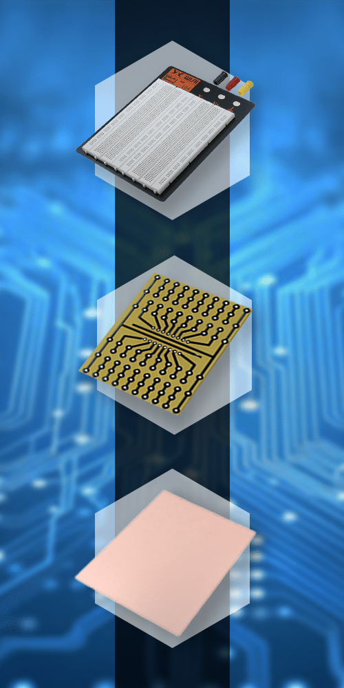
Universal PCBs are laminates with straight traces (or solder pads alone) and holes drilled at a standard spacing (usually 2.54 mm). Electronic components can be attached and soldered to them to facilitate the circuit production. In the case of PCBs with rows of interconnected solder pads, the traces are cut with a knife or reamed – in the case of PCBs that only have holes and solder pads, connections are made by solder bridging.
Since such PCBs are, by their nature, regularly perforated and often made from hard paper (rather than FR4), you can adjust their size to your needs by cutting and breaking, which will speed up your work significantly. However, it should be noted that universal PCBs are available in a wide variety of sizes, often with machine-made fixing holes, so in all likelihood such a treatment will not be needed at all.
 PCB acting as an adapter, designed to work with a variety of SMD components.
A special type of prototype PCBs are multiadapters with pads for mounting components which are housed a specific type of package. They facilitate, among other things, prototyping with the use of surface-mounted components, especially integrated circuits with multiple leads, such as multiplexers, drivers or microcontrollers. They are made in such a way that each SMT pad is connected to at least one THT hole, to which wires or pin headers can be easily soldered.
Prototyping with breadboards
The fastest method for demonstrating and prototyping circuits is to use breadboards. These are flat bodies made of plastic. They have holes at a standard pitch of 2.54 mm on top, suitable for fitting typical THT components. Underneath the holes, there are elongated metal contacts that provide connectivity between all points in each row (each row has a separate set of contacts). The fields placed on the sides of the PCB remain shorted over the entire length of the column, as they have been designed to act as power traces, shared by multiple components. Thanks to this layout, you can produce circuits (even complex ones) without using tools. THT components and connecting wires alone will be enough. Some products are delivered together with such connectors.
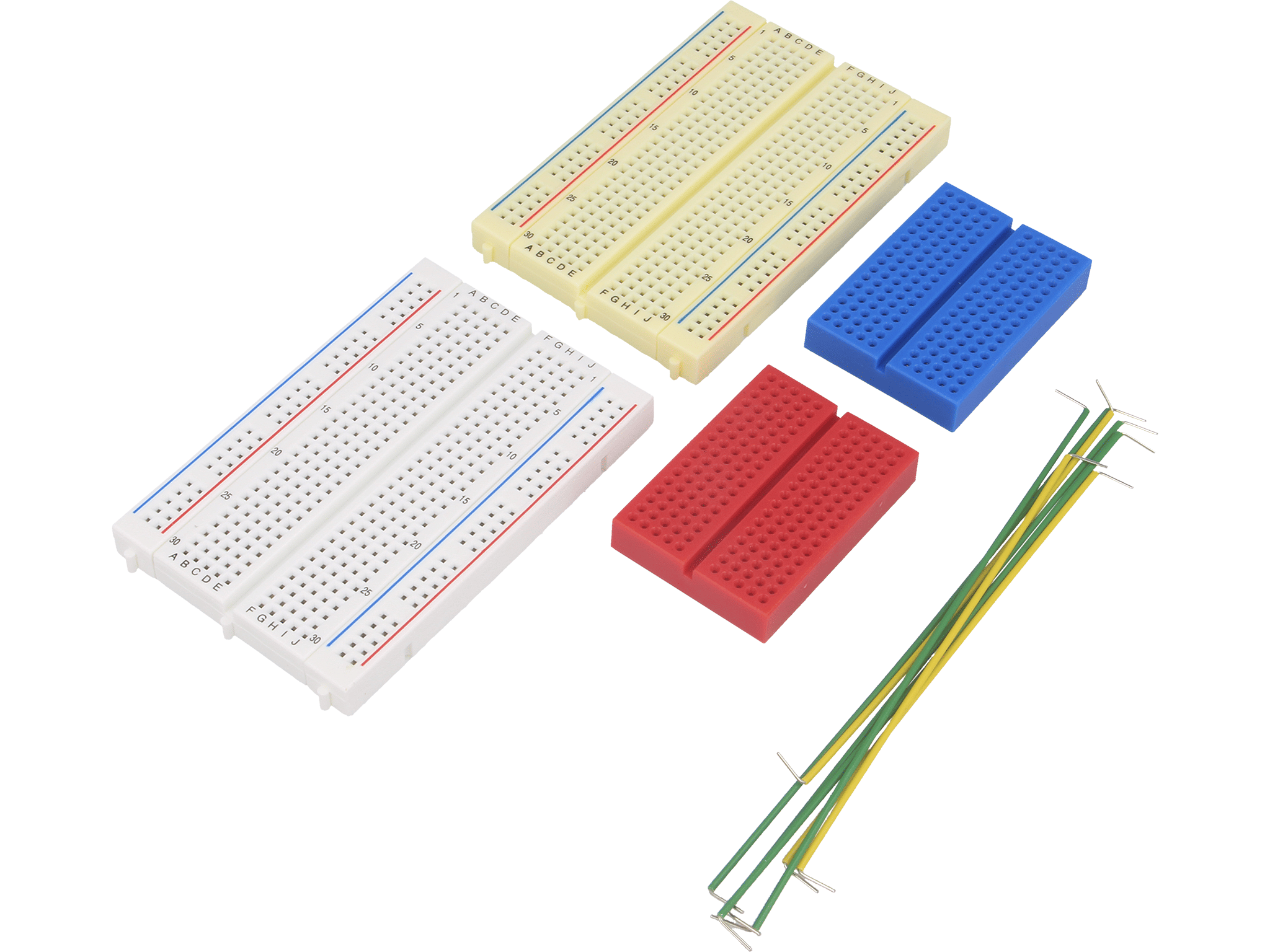 A set of breadboards with a set of connecting cables.
TME offers a wide selection of breadboards – from the smallest (100 fields) to extensive models (3200 fields) placed on a loaded, shielded base and with holes for mounting banana plugs (for easy power connection). Such products are an excellent educational accessory, which invites users to experiment freely with electronics. Nevertheless, professionals are also eager to use them – for example to carry out a quick test of a design solution or to make a temporary replacement circuit. Apart from different sizes, the PCBs can also be distinguished by their colours. What is more, selected models have a modular design and can be connected to form larger boards.
FAQ - Frequently asked questions about laminates and prototype PCBs
How to make a prototype PCB?
PCB prototype can be made in several ways. The most common methods are CNC milling, classic chemical etching or phototransfer technology. Using a CNC milling machine, a digitally controlled tool removes a layer of copper, leaving the circuit paths. Chemical etching involves applying a protective layer to the laminate, after which the laminate is immersed in a chemical solution, which removes the unprotected copper. Phototransfer technology uses photosensitive varnish and UV light exposure, which makes it possible to obtain a very precise image of the circuit even in home conditions.
What is FR laminate-4?
Laminates FR-4 is one of the most popular materials used in the manufacture of printed circuit boards (PCBs). It consists mainly of fiberglass and epoxy resin, which provides high flame resistance (FR stands for "flame retardant"). FR-4 has a favorable strength-to-weight ratio, good electrical insulation and thermal stability, making it an ideal choice for standard electronic applications.
What is the difference between a prototype PCB and a standard PCB?
Prototype PCBs are mainly used to test new electronic designs before they are put into mass production. They are often made in single or small batches, which allows for quick corrections and design optimization. Standard PCBs are produced in larger quantities and according to an established design, which has been thoroughly tested and optimized in advance for mass production.
What are the advantages of using contact boards?
Contact boards allow rapid prototyping of electronic circuits without the need for soldering. Their main advantages are simplicity of use, reusability and immediate change of circuit by simply re-wiring components. They are particularly useful in education, but also used by professionals when testing initial circuit concepts, which significantly speeds up design work.
Does the thickness of PCB laminates matter?
Yes, pCB Laminates thickness is an important factor when designing and manufacturing printed circuit boards. Standard laminates range in thickness from 0,6mm to 2,4mm. Thicker Laminates provide greater mechanical strength and greater tolerance during machining (e.g. milling). Thinner Laminates, on the other hand, may be preferred in applications, where minimization of dimensions is important or flexibility is required, such as. in flexible circuits.
Which PCB prototyping method to choose for precision SMD circuits?
For precision circuits with SMD components, it is recommended to use phototransfer technology. It allows to achieve very high accuracy of paths, reaching up to several micrometers, which is crucial for miniature surface mounted circuits. Laminates covered with photosensitive layer are available as finished products, that allow home or professional fabrication of precise circuits without specialized equipment.
Do aluminum Laminates have advantages over classic laminates?
Laminates made of aluminum are particularly applicable where, where effective heat dissipation is important, such as. in high power systems, lED lighting, or automotive electronics. The aluminum layer acts as a heat sink, improving the thermal efficiency of the circuit. Compared to classical laminates (e.g. FR-4), aluminum provide better temperature stability and extend the life of electronic circuits, working in difficult thermal conditions.
Transfer Multisort Elektronik (TME) is one of the world’s largest global distributors of electronic components, electrotechnical parts, workshop equipment, and industrial automation. The catalog includes over 1,500,000 products from 1,300 leading manufacturers. TME’s modern logistics centers in Łódź and Rzgów (Poland), with a combined area of over 40,000 m², ship nearly 6,000 packages daily to customers in more than 150 countries.
TME also invests in the development of knowledge and skills of young engineers and electronics enthusiasts through the TME Education project, and supports the tech community by organizing the TechMasterEvent series, promoting innovation and experience exchange.